Manufacturing Notes · Inspection and test
What AOI Misses and What X-Ray Cannot See
Every inspection method has a blind side, and the escape risk of a programme is set by the defects that fall into it. This note maps six defects against the method that catches them, then sets out what is left over and how those escapes reach the field.
Published 5 February 2026 · updated 14 February 2026 · 9 min read · Marcus Lim, Test Engineering Lead
The boundaries
Five limits that decide what escapes
Each limit below is a boundary of the method rather than a fault in the machine. They run in a single column, because knowing where the boundary sits is what lets a test strategy be chosen on purpose instead of by habit.
Limit 01
AOI is optical, so it sees surfaces
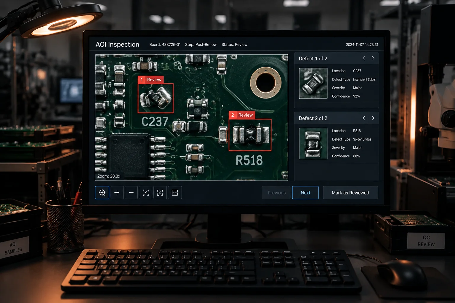
An optical system catches tombstoning, bridging, missing or misaligned parts, wrong polarity and insufficient solder, because every one of those changes the appearance of the joint. It cannot see under a BGA, under a shielded can or under a connector body, which is a hardware boundary and not a resolution problem that a better camera solves. We run 100% AOI coverage on all SMT builds and treat that as the floor, not the ceiling.
Limit 02
X-ray sees structure, not electricity
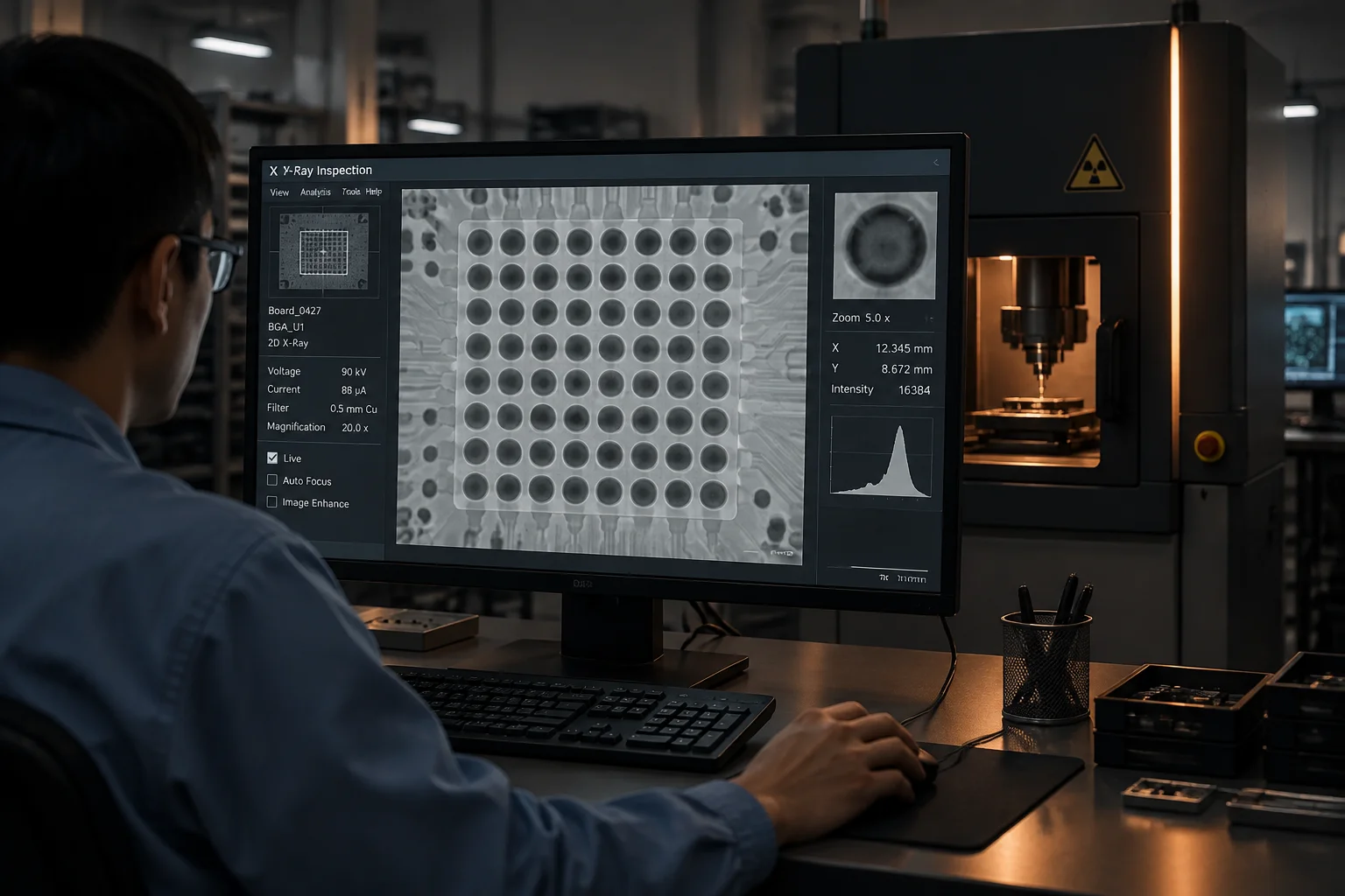
Two-dimensional and three-dimensional X-ray shows voids, head-in-pillow, ball integrity and barrel fill through the package. It says nothing about whether the circuit works: a joint with 8% voidage and a cracked die both look like a joint. X-ray is the only practical way to inspect a ball grid array, and it still has to be paired with an electrical test to mean anything.
Limit 03
Visual inspection is a thin filter
Human visual inspection at the bench catches what is obvious and misses what is small. Below a 0.4 mm leaded or 0.35 mm leadless pitch, and at 01005 chip size, the eye adds little that AOI has not already covered. Visual inspection earns its place on mechanical items, labelling and packaging, where a camera has no advantage.
Limit 04
ICT finds opens, not marginal joints
In-circuit test proves continuity and value, and finds the open circuit or the wrong component. A joint that is mechanically intermittent passes an ICT probe push-down and fails in a thermal cycle six months later. This is where the classic escape lives: the board passes every gate and the field return rate does the discovery instead.
Limit 05
Only functional test proves behaviour
Functional test is the slowest and most expensive method per unit, and it is the only one that confirms the assembly does what the customer's product needs it to do. It catches what AOI and X-ray structurally cannot, which is why the coverage rule is additive: AOI, X-ray, ICT and functional test are chosen per programme by escape risk and volume, never by habit.
Defect atlas
The defect atlas: six failures and the method that catches each
Six defects that account for the majority of process escapes, with the method that catches each one and the escape risk that remains after that method has run.
DEF-01
Tombstoning
- Caught by
- AOI
Escape risk low: the part lifts clear of its pad, so the height change is visible. Where a tombstone sits under a shield can, the risk moves to high and only functional test finds it.
DEF-02
Solder bridging
- Caught by
- AOI, then ICT
Escape risk low on exposed leads, high between fine-pitch pins under a body. ICT closes most of the remaining gap by proving continuity between the pins.
DEF-03
Insufficient solder
- Caught by
- AOI by volume estimate
Escape risk medium: a fillet that is thin but present passes an optical volume check. A thin fillet on a heavy thermal pad survives the bench and cracks in the field.
DEF-04
BGA voiding
- Caught by
- X-ray, 2D or 3D
Escape risk medium: acceptance is under 25% void for Class 2 and under 10% for Class 3, and a void inside the band is released by rule. Voids near the band edge are the ones that grow under thermal cycling.
DEF-05
Head-in-pillow
- Caught by
- X-ray, 3D only
Escape risk high: the ball touches the paste without coalescing, so 2D X-ray shows a joint that is not bonded. It survives a bench test and fails after a few thermal cycles.
DEF-06
Missing or wrong part
- Caught by
- AOI, then functional test
Escape risk low for a missing part, higher for a wrong value when the package is identical to the correct one. Functional test resolves both where the limits are written correctly.
Combined coverage
Where each method stops, drawn across one panel
Optical and transmission imaging answer different questions about the same joint. Putting the two together on one panel is the cheapest way to see the gap that remains, and to decide which defects the programme can afford to carry.
Escape risk
Escape risk by defect, and where the escape surfaces
Ten defect and test combinations, with the physical reason the method is limited and the stage at which a miss normally becomes visible. The last column is the one that matters commercially: an escape found in the field costs a return, a freight leg and a customer conversation.
| Defect | Physical limit | Escape risk | Surfaces at |
|---|---|---|---|
| Bridging under a body | No line of sight to the joint | High without ICT | ICT or functional test |
| Insufficient solder fillet | Thin fillet still passes a volume check | Medium | Thermal cycling in the field |
| BGA void near the limit | Released inside the 25% Class 2 band | Medium | Field return after cycling |
| Head-in-pillow | Ball contacts paste without coalescing | High on 2D X-ray only | Fatigue crack in the field |
| Open barrel on a plated hole | Fill level hard to measure optically | Medium | Functional test or field |
| Wrong value, same package | Optically identical to the correct part | High without a limit set | Functional test |
| Wrong polarity on a diode | Cathode marking small at 0402 | Low at AOI | AOI |
| Popcorning after moisture uptake | Internal delamination invisible to AOI | High without MSL control | C-SAM or the field |
| Intermittent press-fit joint | Passes probe contact pressure | Medium | Vibration test or field |
| Wrong grade of a correct part | Same marking, different temperature rating | High | Temperature cycling in the field |
Escape risk is the residual exposure after the stated method has run at its published acceptance limits, not a defect rate. Published programme data for reference: 0.42% DPMO on SMT placements, 0.06% field return rate, 99.4% first-pass yield.
Reader questions
Questions that follow the atlas
Rarely. Screen it where a plated through-hole barrel must be filled, where a QFN has a large thermal pad, or where the programme is Class 3 and the escape risk justifies the scan time. For a board that is entirely surface-mount with exposed leads, AOI plus functional test covers the same ground at a lower cost per unit.
Under 25% for Class 2 and under 10% for Class 3 is the usual band, and it is normally written per ball rather than per package. Ask for the measurement method as well as the number: 2D and 3D X-ray report different void figures on the same joint, so a specification that names the limit but not the method creates disputes.
No, and the reason is economic rather than technical. Functional test catches defects that optical and transmission methods miss, but it is the slowest and most expensive method per unit and a marginal joint can pass it once and fail later. The methods are additive: removing a cheap gate to save time moves the cost into returns.