DFA-01 / Land pattern
Pad geometry from a named density level
We build to IPC-7351B density level B unless your CAD library says otherwise, keeping the pad-to-pad gap at 0.2 mm or more so a 01005 part cannot bridge during reflow.

SMT assembly / 01005 to 0.35 mm pitch
Chip shooters place 01005 and 0201 passives at 40,000-80,000 components per hour while flexible placers index to +/-15-25 um for 0.35 mm leadless packages. Paste is printed through a laser-cut stencil, reflowed in a 10-zone oven against a profile validated for that board, and inspected with 100% AOI plus X-Ray on every hidden joint.
Process
Four variables decide whether a 0.35 mm pad array yields: the placement head, the vision system, the paste volume and the thermal profile. Each of them is measurable on the line.
The three high-speed lines run chip shooters at 40,000-80,000 CPH for passives down to 01005, while three high-mix lines run flexible placers at 3,000-8,000 CPH for connectors, shields and fine-pitch ICs on the same board.
Ultra-fine-pitch mode drops to +/-15-25 um using on-the-fly vision and coplanarity checks, with flux dipping for 0.35 mm leadless parts. That mode costs $0.10-0.50 per micro-BGA placement and always carries X-Ray.
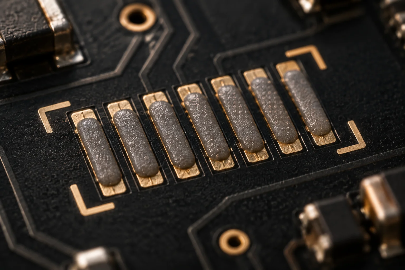
Stencil foil is chosen per pitch: 100 um below 0.4 mm, 120 um for standard mixed builds and 150 um over large thermal pads. A 50 x 100 mm assembly consumes 0.5-1.5 g of Type 4 or Type 5 paste, printed and verified by SPI before the first component is placed.
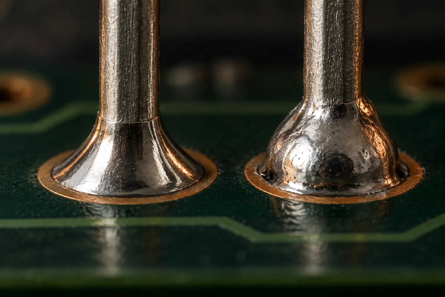
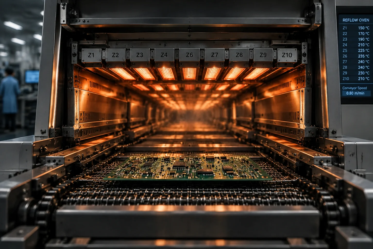
SAC305 reflows at a 217 C liquidus. The 10-zone forced-convection oven holds a soak or ramp-to-spike profile specific to the board, keeping ramp under 3 C per second and time above liquidus inside a 45-75 second window.

Capability table
Every row is a setting an engineer can verify on the line or in the process record, not a marketing figure.
| Parameter | Machine class or method | Capability | Governing standard |
|---|---|---|---|
| Minimum chip size | Chip shooter, high-speed head | 01005 (0.4 x 0.2 mm) and 0201 passives | IPC-7351B land patterns |
| Minimum leadless pitch | Flexible placer, vision alignment | 0.35 mm BGA, micro-BGA, QFN and CSP | IPC-7095 |
| Minimum leaded pitch | Flexible placer | 0.4 mm QFP, TQFP and SOIC families | J-STD-001 |
| Accuracy, fine-pitch mode | Vision alignment with flux dipping | +/-15-25 um at 0.35-0.4 mm pitch | J-STD-001 Class 3 |
| Accuracy, chip-shooter mode | High-speed rotary head | +/-30-50 um at full speed | Process capability study |
| Throughput, passives | Chip shooter | 40,000-80,000 CPH | Per-line capacity plan |
| Throughput, fine-pitch ICs | Flexible placer head | 3,000-8,000 placements per hour | Per-line capacity plan |
| Micro-BGA placement cost | Ultra-fine-pitch mode | $0.10-0.50 per placement, X-Ray mandatory | Industry-typical band |
| Solder paste | Type 4 standard, Type 5 below 0.4 mm | 0.5-1.5 g per 50 x 100 mm assembly | J-STD-005 powder grade |
| Stencil foil | Laser-cut, nano-coated | 100 um below 0.4 mm, 120 um standard, 150 um thermal pads | Aperture area ratio above 0.66 |
| Reflow oven | 10-zone forced convection | Soak and ramp-to-spike profiles per part number | Profile validated per design |
| Alloy and liquidus | SAC305 lead-free | 217 C liquidus, peak 235-245 C | J-STD-001 alloy control |
| Double-sided builds | UV and thermal-cure adhesive dots | $0.01-0.03 per heavy bottom-side component | Second-pass profile review |
| BGA void acceptance | 3D X-Ray on 100% of joints | Below 25% Class 2, below 10% Class 3 | IPC-7095 |
| Panelisation | 2-up and 4-up multi-image panels | 5 mm minimum rail for AOI clearance | IPC-7351B panel rules |
| Ionic contamination | ROSE and ion chromatography | 1.56 ug NaCl/cm2 Class 2, 0.78 ug Class 3 | IPC-A-610 cleanliness |
Design for assembly
These are the rules the DFM team applies before a stencil is cut. Failing one is not a rejection; it is a conversation with a number attached.
DFA-01 / Land pattern
We build to IPC-7351B density level B unless your CAD library says otherwise, keeping the pad-to-pad gap at 0.2 mm or more so a 01005 part cannot bridge during reflow.
DFA-02 / Stencil ratio
A 0.4 mm pitch device needs an aperture area ratio above 0.66 to release paste consistently. Where the ratio falls short, the foil drops to 100 um and the aperture is modified rather than accepted.
DFA-03 / Paste volume
Solder paste inspection verifies deposited volume against the aperture at 80-120%. Printing faults are corrected on the printer instead of being reflowed into a hundred hidden joints.
DFA-04 / Component spacing
Keep 0.3 mm or more between 0402 bodies and 1.0 mm around a QFN. Rework access is what decides whether a single fault costs one joint or one board.
DFA-05 / Fiducials
Three 1.0 mm global fiducials clear of the panel rail, plus two local fiducials per fine-pitch device. Without them the vision system aligns to the panel, not to the part.
DFA-06 / Panel design
A 5 mm minimum rail and 2.0 mm breakaway tabs keep the panel stable through printing, placement and reflow. Below that, edge components see more vibration than the process window allows.
DFA-07 / Thermal relief
A 0402 pad tied straight into a ground plane sinks heat and starves the joint. Use 0.25 mm spokes or thermal relief so both ends of the part reach liquidus together.
DFA-08 / Tombstoning
On 01005 and 0201 parts, mismatch between the two pad areas or their thermal paths lifts one end. We check pad area and copper balance to within 10% before releasing the stencil.
DFA-09 / Test access
A 1.0 mm test pad on a 2.54 mm grid, kept 3 mm clear of tall components, is what makes ICT or flying probe possible later. Test access designed at layout costs nothing; retrofitted it costs a revision.
DFA-10 / Second side
Any bottom-side part above roughly 3 g needs adhesive dots before the second reflow, at $0.01-0.03 per component. Mass, not size, is what drops a part into the oven.
Reflow profile
The oven profile is validated on the actual assembly, because a 0.6 mm wearable and a 3.2 mm power board do not share a thermal curve.
soak      150-180 C      60-90 s     measured 74 s        PASS
ramp      max 3 C/s      limit        measured 2.1 C/s     PASS
peak      235-245 C      limit        measured 239 C       PASS
TAL       above 217 C    45-75 s      measured 62 s        PASS
delta     cold to hot spot   max 12 C   measured 9 C
BGA void  Class 3 limit 10%   measured 4.8%             PASS
stencil   120 um        paste Type 4    SPI 108% of aperture
note      2 heavy shields on bottom side, adhesive dots applied before pass 2
Macro record
Three views of the same capability: paste on the pad, the joint after reflow, and the finished double-sided assembly.
Questions
Yes. 01005 and 0201 passives run on the same chip-shooter programme as 0402 parts, so placement stays at $0.005-0.015 per passive. The premium starts at 0.35 mm leadless pitch, where a micro-BGA placement costs $0.10-0.50 and X-Ray becomes mandatory.
0.35 mm leadless on BGA, micro-BGA, QFN and CSP, and 0.4 mm on leaded packages. Below that the paste volume and stencil area ratio stop supporting a repeatable joint, so the design is flagged in DFM rather than quoted.
Every BGA and QFN goes through 3D X-Ray for void percentage, ball integrity and head-in-pillow, measured against the IPC-7095 limit of 25% at Class 2 and 10% at Class 3. AOI covers what is visible; X-Ray covers what is underneath.
Seven fields. A process engineer replies within one working day.
Seven fields. A process engineer replies within one working day.
Seven fields. A process engineer replies within one working day.