| Trace width and spacing |
0.15 mm minimum on 1 oz copper; 0.10 mm only where the layout cannot avoid it |
Etch tolerance is a fixed percentage of the copper thickness, so a narrower trace loses a larger share of its width to the same process variation |
Open circuits at the etch step and a bare-board price 25 to 40% higher, with the yield loss carried on every panel of the order |
| Annular ring |
0.20 mm minimum on a plated through hole; 0.15 mm on a via with a 0.30 mm drill |
The ring is what survives drill wander; below the minimum the hole breaks out of the pad on one side |
Intermittent barrel-to-pad opens that pass AOI and fail thermal cycling in the field, which is the most expensive place to find them |
| Minimum drill and via |
0.20 mm finished via, 0.25 mm for a via in a thermal plane |
Aspect ratio is what limits plating throw; a deep small hole plates thin copper in the barrel middle |
Marginal barrel plating, barrel cracks after thermal cycling and a repair that cannot be reworked |
| Stencil aperture area ratio |
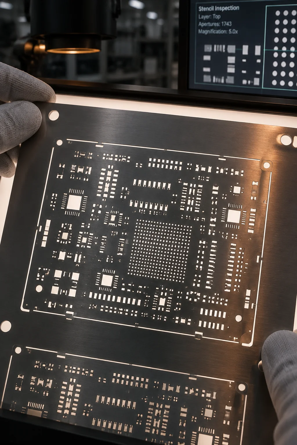
0.66 minimum, where area ratio is aperture area divided by aperture wall area |
Below that figure the paste releases poorly from the stencil wall and the deposit is short and uneven |
Insufficient paste on fine-pitch pads, which shows up as opens and weak joints after reflow rather than at print |
| Stencil thickness |
100, 120 or 150 um foil, chosen from the finest pitch on the board |
Deposited paste volume is area multiplied by thickness, so thickness sets the volume for every joint on the board at once |
Bridging where the paste is too thick for the pitch and starved joints where it is too thin for a heavy thermal pad |
| Component-to-component clearance |
0.30 mm between 0402 and smaller bodies, measured at the body and not the pad |
Placement accuracy on a chip-shooter is plus or minus 0.05 mm, and the nozzle and feeder tolerances add to it |
Tombstoning from unequal paste deposits, part-to-part contact after reflow, and design rules that stop the assembly being inspected |
| Courtyard and keep-out |
IPC-7351 nominal courtyard on every part, with no via or test pad inside it |
Placement, rework and inspection all need physical access to the part that a courtyard reserves |
Irreparable assemblies where a part cannot be removed without damaging a neighbouring one |
| Thermal relief on planes |
0.25 mm spoke width with four spokes on through-hole and heavy pads |
A pad connected to a plane by solid copper cannot reach reflow temperature with the rest of the joint |
Cold joints and voiding on power devices, and hand rework on a joint that should have soldered in the oven |
| Via-in-pad |
Filled and capped or plated over, never an open via inside a paste aperture |
An open via below a pad drains the paste deposit into the barrel during reflow |
Solder starvation and voids under the device, on the packages where rework is least possible |
| Through-hole land |
0.25 mm annular ring and 0.60 mm pad-to-pad spacing at the wave |
Wave soldering needs a solder shadow-free path and enough land to form a fillet |
Solder bridging between adjacent pins and insufficient fill on a connector row that has to carry current |
| Test point access |
100 test points maximum, 1.0 mm pads on a 2.54 mm grid |
Probe count and pitch decide the fixture cost, and fixture cost is a fixed charge against the programme |
An in-circuit fixture priced at the top of the 2,000 to 50,000 USD band, or a board that can only be tested by flying probe |
| Fiducials |
1.0 mm copper dot with a 2.0 mm clear area, three per panel and two per fine-pitch block |
Global fiducials locate the panel; local fiducials correct the placement of a fine-pitch device that global alignment cannot hold |
Placement offset across the panel and a first-article rejection that repeats on every panel until the fiducials are added |
| Panelisation |
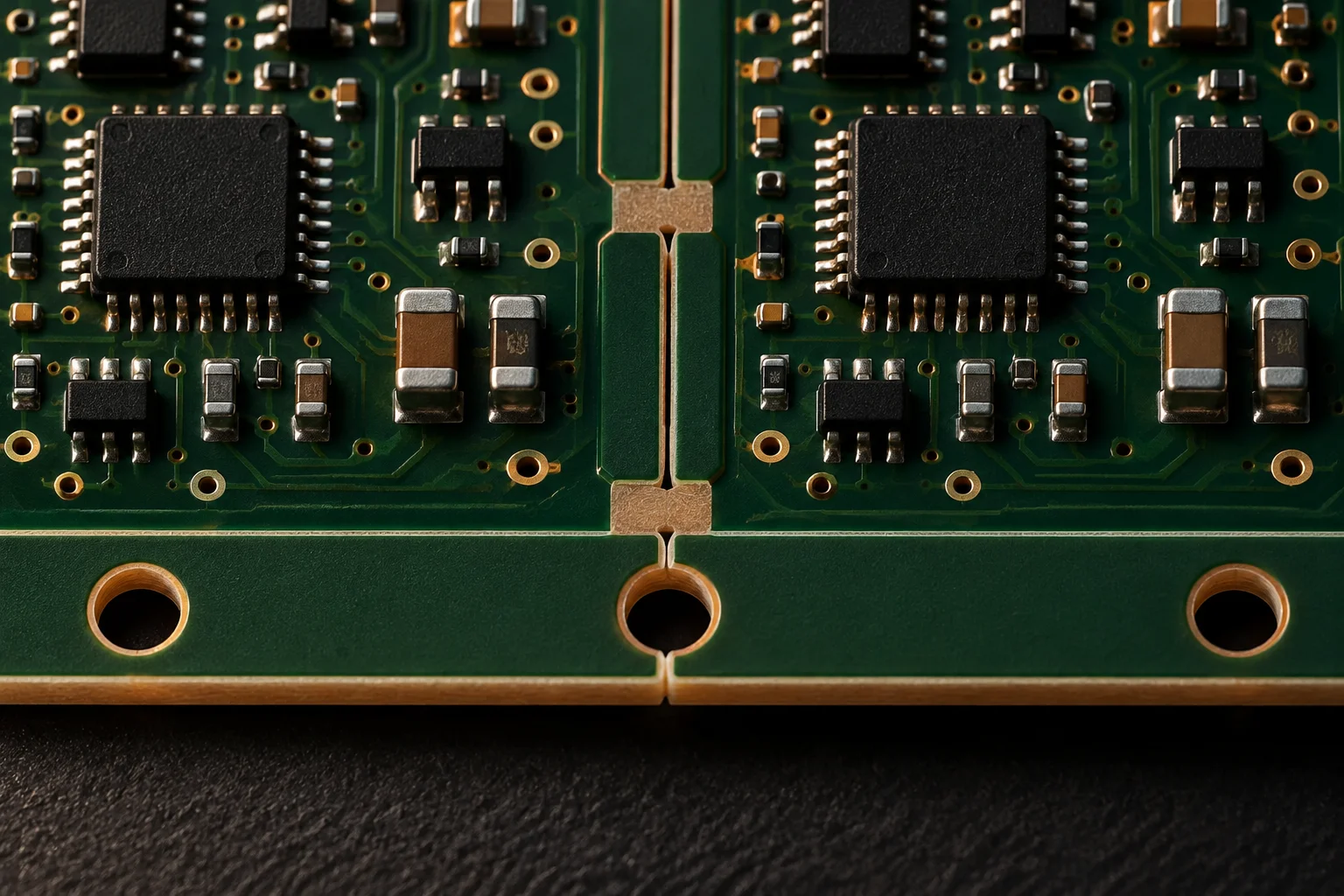
5 mm breakaway rails with mouse-bites or V-score on a 300 x 250 mm carrier as a starting point |
Assembly is priced per panel, so board count per panel sets the machine time each unit absorbs |
Placement cost per unit 20 to 30% above a well-nested panel, and board edge damage where the rails are too thin |
| Silkscreen over pads |
No legend inside a paste aperture, and no reference designator smaller than 0.8 mm |
Ink on a land reduces the wettable area and can lift into the joint during reflow |
Solder balls and poor wetting on the affected pads, plus inspection ambiguity when a designator is unreadable |